This FPGA-based motherboard, part of the WARP project, is the central processing platform for prototyping and deploying wireless communications research. The modular system connects to RF interfaces to create a single 4-radio board capable of implementing next generation wireless algorithms. The board was designed and hand-routed as part of my M.S. thesis.
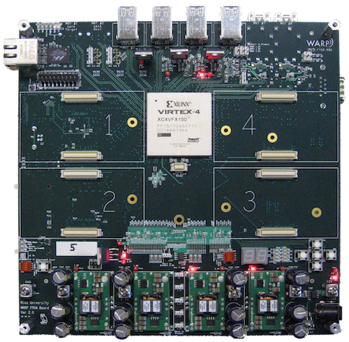
Some features of this 8in x 8in board design are:
- A 1517-pin Xilinx Virtex-4 FX100 FPGA, the largest production Virtex-4
- 18 copper layers for power distribution and signal routing
- Utilization of all 768 I/O available on the Virtex-4
- RF and analog data interfaces as part of a modular daughtercard standard, drawing power and I/O resource from the FPGA
- RF and logic clocks distributed from a central clocking board enabling syncing of multiple RF interfaces
- Multiple debug and data source interfaces for quick reprogramming, real-time debug and high bandwidth (3 Gigabit Ethernet) data input
- Up to 4GB and 64-bit wide bus of DDR2 SO-DIMM Memory where each byte-group is length-matched to within 1mil on the board, minimizing the phase difference between groups with a custom termination scheme.
- High-speed serial links (50 ohm impendence-matched differential pairs) sustaining data rates up to 6.25Gbps
The Backdoor Board is an add-on to the FPGA Board and enables fine-grained network monitoring of experimental algorithms over a large node network. This board was also developed as part of my M.S. thesis. Some features of this 5.4in x 2.5in board are:
- The ability to control, update and monitor the experimental algorithms running on the FPGA Board
- Two processors: an Axis ETRAX microprocessor in a multi-chip module and a Xilinx Spartan-3AN FPGA to manage interaction and add robustness
- 8 copper layers on the board, 4 for routing and 4 for power
- Three remote communication interfaces connecting to both processors for redundancy and no service interruption
- Flash image storage for both processors ensuring successful startup even during power glitches
This is a commercially available daughtercard to the FPGA Board for the WARP project. It is debug and test interface when prototyping a 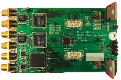 custom physical layer design in the FPGA. Some features of this daughtercard are:
- 4 channels of Digital-to-Analog conversion and 2 channels of Analog-to-Digital conversion
- Output channels to view real-time baseband QAM constellations
- Input channels to be used as data sources without RF interference
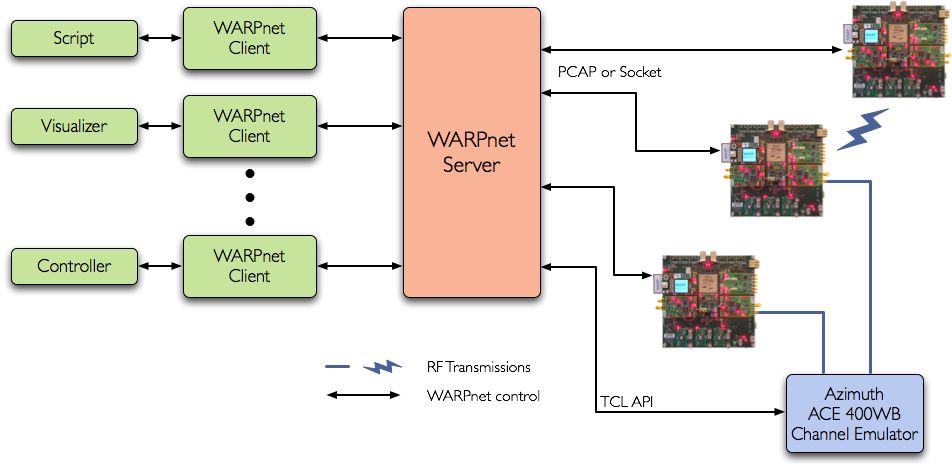
The WARPnet Control Framwork is an Object Oriented Python architecture that enables real-time control of a network of WARP FPGA boards. Some of its architectural features are:
- A server-client architecture in Python running in a UNIX environment
- Use of the Twisted networking library for connection management and custom code to manage all clients
- Server handling of all requests from clients (scripts, visualizers, mobile devices) and relaying of all responses from any number of WARP FPGA Boards
- FPGA Boards can connect over raw PCAP or socket connections
- FPGA code enables control of low-level physical and MAC layer registers
- Logging of fine-grained performance metrics to scripts or visualizers in real-time
- Characterization of physical/MAC layers is the primary use-case where a host of parameters can be swept over several days to build a complete matrix of performance
